
Critical Dimension Metrology
and Scatterometry
Our patented technology enables us to inspect the quality of gratings and thin films used in photonics, semiconductors, and quantum technologies. Using this technology, we can determine modifications of geometrical parameters and optical properties during the fabrication of nanostructures in a contact-free and non-destructive manner.
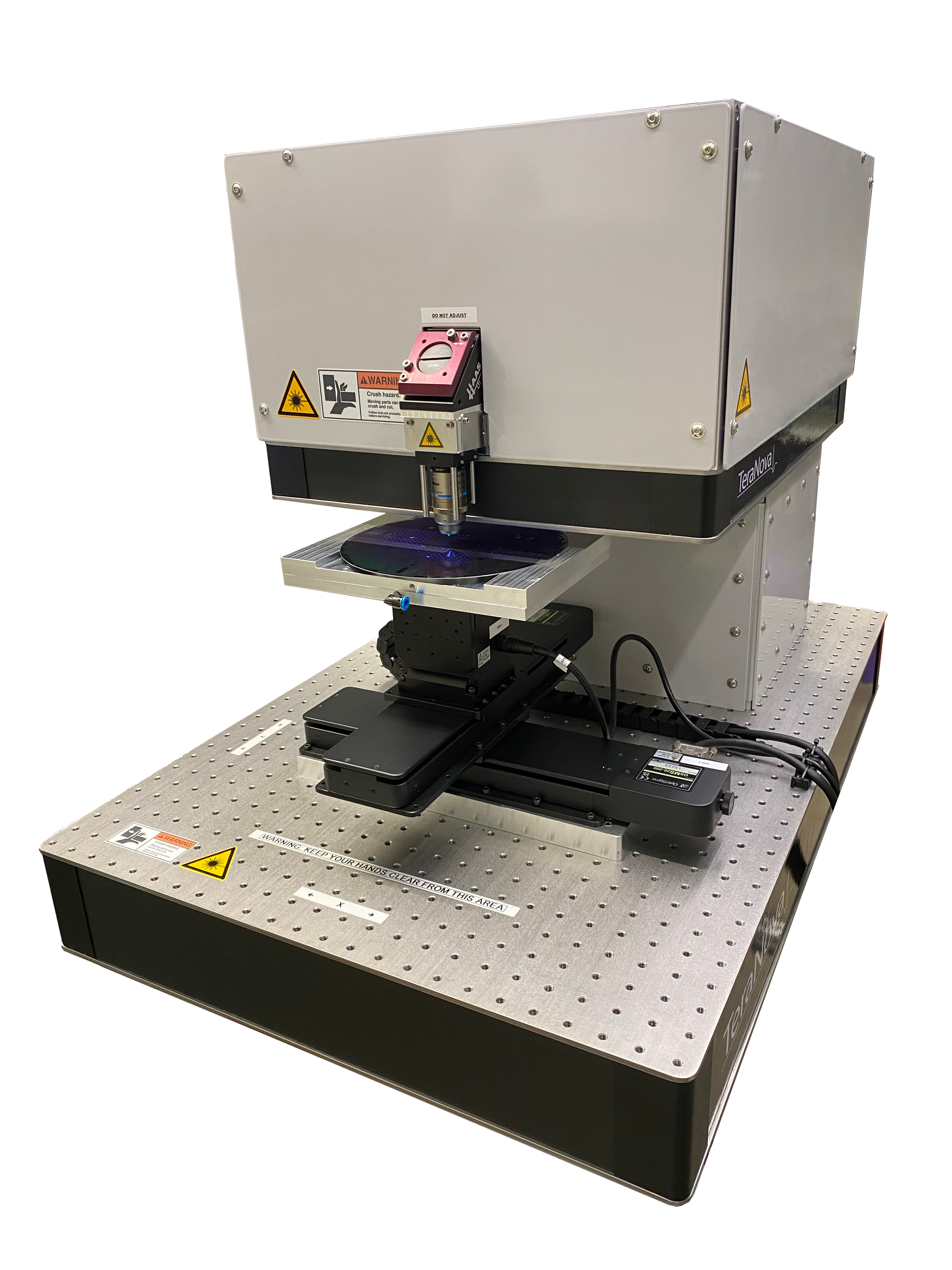
LabScatter
Critical Dimension Metrology and Scatterometry for Gratings and Thin Films
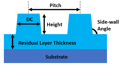
This instrument is based on the principles of Fourier microscopy with collimated illumination that allows us to collect the intensity of diffracted and reflected light simultaneously. Using this technique, we extract crucial information such as grating pitch, height, width/diameter, residual layer thickness, side wall angle, and refractive index in a comprehensive manner, all at the same time.
Features:
- Single-nanometer resolution, sensitivity, and reproducibility
- Low cost and compact footprint (1000 x 700 mm2)
- High throughput
- Substrate independent (semiconductor, metal, glass, diamond, etc.)
- Compatible with all wafer / substrate sizes
- Intuitive operation equipped with fully automatic software package
Contact us for questions related to your applications or for demonstration trials.
Technology Principle
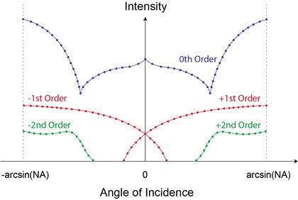
By scanning the angle of incident on the surface of a sample, we determine intensity of reflected beam and / or diffracted orders at each incident angle and for a given polarization (TE and / or TM). An illustrative example of such a measurement for a grating is shown in the figure below. Minor modifications in samples such as geometrical changes, refractive index variations or inhomogeneities in the substrate will affect the measured curves significantly. By fitting such curves, we extract geometrical parameters and refractive indices of the measured samples.
Explore Measurement Tutorials and Capabilities

info@teranova.nl
+31 62 819 28 20
TeraNova BV, Flux Building (office 1.116),
Groene Loper 19, 5612AP, Eindhoven, The Netherlands
KvK number: 75646285 - VAT number: NL860351518B01

Copyright © All Rights Reserved - 2024