Terahertz Spectroscopy
for Materials Characterization
Examples:
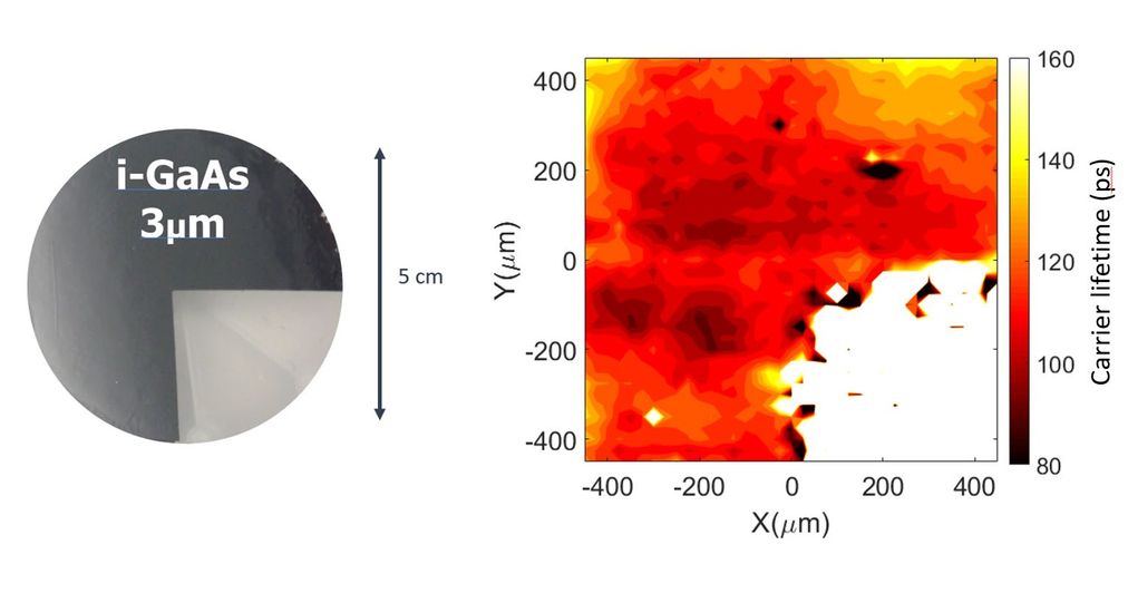
(Left) Photograph of an epitaxially grown GaAs layer. The right-low quarter of the layer has been removed for referencing. (Right) Carrier life-time map obtained by photo-excitation the GaAs layer at 800 nm and measurements of the THz near-field transmission. The carrier life-time map is taken in area of 1 mm x 1 mm at the center of the sample.
Terahertz Time-Domain Near-Field Microscopy
High-spatial resolution THz near-field microscope. The THz microscope allows to measure the THz radiation transmitted through a sample at the surface with a scanning near-field probe. By using near-field detection, this setup overcomes the main limitation of THz spectroscopy, i.e., the spatial resolution. The combination of THz near-field microscopy with optical pump provides a unique instrument for the investigation of the transient photo-conductivity and the carrier life-time of photo-excited semiconductors.
This technology has been developed with financial support of the European Research Council through the ERC- Proof of Concept grant (MicroMap, grant number 665619).
Features
- THz bandwidth: 0.07 – 1 THz
- Scanning area: 1 cm2
- Spatial resolution: appr. 25 μm
- Excitation wavelength: 400 – 1000 nm
- Time resolution: 100 fs
- Possibility of detecting electric field components along x, y and z directions
More information about our THz nearfield microscope can be found below.


